Neuromorphic X1
Neuromorphic X1
Overview
Neuromorphic X1 is a compact and efficient analog in-memory compute macro designed for next-generation edge AI applications. Built on a 32×32 1T1R crossbar array, it leverages analog weights to perform multiply-accumulate operations directly in memory, minimizing data movement and maximizing energy efficiency.
With integrated decoders and sense amplifiers, the X1 macro delivers 1kb of analog weight storage in a compact 0.28 mm² area. Its Wishbone bus compatibility ensures seamless integration into digital SoCs, including Caravel-based platforms.
Key Features
- In-Memory Compute: Efficient analog MACs for AI workloads
- Compact Footprint: 0.28 mm² including peripheral circuitry
- Wishbone Interface: Easy integration with standard digital buses
- Ready for Tapeout: Fully synthesized and foundry-compatible
Neuromorphic X1 enables AI processing at the edge with ultra-low power and area, making it ideal for sensor-rich, power-constrained environments.
Installation
See the detailed information for the base macro here
Integrate our IP on chip foundry platform here
Memory Features
- Synchronous Read / Write cycles (single-clock timing)
- Active-high bit enables for per-lane writes
- Single R/W control
— 0 = Write, 1 = Read / Compute - Bit-level (1 T 1 R) programming & verify for precise analog weights
- Separate DI / DO pins to support simultaneous sense & program operations
- Split power rails — core array vs. digital periphery
- Body-bias pins for leakage control and conductance trimming
- Full scan-chain test mode covering address, data & control logic
- Wafer-level burn-in test mode for early-life reliability screening
- Global word-line-OFF option (all WLs clamped when inactive)
- Macro power-switch hooks for deep-sleep isolation
- Clock-gating throughout periphery to minimize dynamic power during idle
Block Diagram
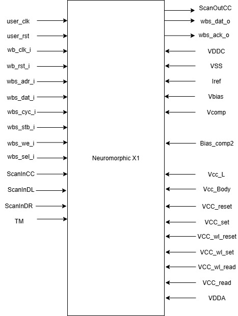
Pin Description
| Name | Type | Direction | Description |
|---|---|---|---|
user_clk |
DIGITAL | IN | Clock synchronizes the operations of the memory. All inputs are sampled on rising edge of clock. |
user_rst |
DIGITAL | IN | This is the reset pin, which is active low. Reset is applied when this pin is low, and deasserted when the pin is high. |
wb_rst_i |
DIGITAL | IN | Wishbone reset input, active low. Reset is asserted when this pin is low , and released when pin is high. |
wb_clk_i |
DIGITAL | IN | Wishbone clock input. All bus signals are sampled on the rising edge of this clock. |
wbs_adr_i[31:0] |
DIGITAL | IN | This is the wishbone address input pin. When the value on this pin is 32'h3000_0004, the read or write operation starts; otherwise, no action is taken. |
wbs_dat_i[31:0] |
DIGITAL | IN | This is the data input bus. Data is written into the memory location specified by the address bits of this register during a write cycle |
wbs_ack_o |
DIGITAL | OUT | Output acknowledge signal. Asserted high by the slave to indicate the completion of a Wishbone bus cycle (read or write). |
wbs_cyc_i |
DIGITAL | IN | Input cycle signal. Asserted high by the master to indicate that a valid bus cycle (read or write) is in progress. |
wbs_stb_i |
DIGITAL | IN | Input strobe signal..Asserted high by the master to indicate a valid data transfer request (read or write) to the slave. |
wbs_we_i |
DIGITAL | IN | Input write-enable signal.When pin is low it performs a write operation. When the pin is high it performs a read operation. |
wbs_sel_i[3:0] |
DIGITAL | IN | These are input pins. To perform a read or write operation, SEL must be 4'b0010 |
wbs_dat_o[31:0] |
DIGITAL | OUT | During a read operation (wbs_we_i = 0), this pin carries data from memory. |
ScanInCC |
DIGITAL | IN | Scan enable input pin. When asserted high, the scan chain is activated, allowing serial test data to be shifted through for scan-based testing. When deasserted low, the scan chain is disabled, and the module operates normally in its functional mode. |
ScanInDL |
DIGITAL | IN | This pin is the input to the data scan chain for the user-clock-specified design. When the scan mode is enabled via the scan enable signal, serial test data is shifted into the module through this pin for scan-based testing. |
ScanInDR |
DIGITAL | IN | This pin is the input to the data scan chain for the Wishbone-clock-based design. When scan mode is enabled via the scan enable signal, serial test data is shifted into the module through this pin for scan-based testing. During normal functional operation, this pin remains inactive. |
TM |
DIGITAL | IN | When TM (Testmode)is high, memory is in testmode and normal memory operation is disabled. Inputs are tied to outputs through scan chain logic. |
ScanOutCC |
DIGITAL | OUT | output of scan chain of data input pins. |
Iref |
ANALOG | IN | 100 µA DC current reference input; provide a quiet, low-noise source to bias internal analog circuits. |
VSS |
ANALOG | IN | 0 V analog ground reference. |
Vcc_read |
ANALOG | IN | 0.3 V read rail. |
Vcomp |
ANALOG | IN | 0.6 V comparator/reference bias input. |
Bias_comp2 |
ANALOG | IN | 0.6 V comparator bias input. |
Vcc_wl_read |
ANALOG | IN | 0.7 V wordline read rail. |
Vcc_wl_set |
ANALOG | IN | 1.8 V wordline set rail. |
VDDA |
ANALOG | IN | 1.8 V analog supply. |
VDDC |
ANALOG | IN | 1.8 V analog core digital supply. |
Vbias |
ANALOG | IN | 1.8 V analog bias input. |
Vcc_wl_reset |
ANALOG | IN | 2.6 V wordline reset rail. |
Vcc_set |
ANALOG | IN | 3.3 V array “set” rail. |
Vcc_reset |
ANALOG | IN | 3.3 V array “reset” |
Vcc_L |
ANALOG | IN | 5 V for level shifter. |
Vcc_Body |
ANALOG | IN | 5 V body-bias supply. |
Specifications
DC Specifications
Conditions
- Process Condition : Typical
- Junction Temperature : 25.000 deg C
- Operating Voltage : 1.800 V
- Operating Frequency : 50 MHz
Power Dissipation When R_WB=HIGH Note:- read enable , which is active low pin
- READ Active = 77.566 pJ
- READ Active = 8.618 mA
- READ Peak = 80.613 mA
Power Dissipation When R_WB=LOW Note:- Write enable , which is active low pin
- WRITE Active = 69.948 pJ
- WRITE Active = 7.772 mA
- WRITE Peak = 79.072 mA
Power Dissipation When EN=LOW, All Other Inputs Switching Note:- After providing the address , data inputs but IP is off , if EN is low then this dissipation will occur
- Standby = 0.174 pJ
- Standby = 0.019 mA
- Standby Peak = 0.470 mA
Power Dissipation When TM=HIGH, Clock Switching Note:- This will not be considered bcoz scan insertions are not there
- Test Mode = 9.603 pJ
- Test Mode = 1.067 mA
- Test Peak = 33.687 mA
Leakage: Power switches ON, Disabled (EN=LOW) Note:- when mc , decoder, subtractor is disabled but still there is some power dissipation when EN is LOW
- Power = 41611.200 pW
- Current = 23.120 nA
Leakage - One or More Power switches OFF (VPWRPC=HIGH or VPWRAC=HIGH)Note :- Different modes of MUX are off and Decoder power supply VDD
- Power = 1420.430 pW
- Current = 0.790 nA
Write Voltage Requirements
During memory program operations, an internal high-voltage supply (Vpp) of up to 5V is required for resistive switching in the memory array. This voltage is only active during write pulses and is disabled during read or standby operations.
| Parameter | Symbol | Min | Typ | Max | Unit | Notes |
|---|---|---|---|---|---|---|
| Write Programming Voltage | Vpp | 3.0 | 4.0 | 5.0 | V | Internally or externally generated |
| Write Pulse Width | Twpp | -- | 1.0 | -- | ms | Duration per row write (e.g., 32x32 cells) |
| Vpp Enable Time Before Write | Tvpp_en | 10 | 20 | -- | µs | Time before write strobe to apply Vpp |
| Vpp Disable Time After Write | Tvpp_dis | -- | 10 | 20 | µs | Time after write completes before shutdown |
| Write Voltage Tolerance | ΔVpp | -5% | -- | +5% | -- | Relative to nominal Vpp |
Operating Voltages by Mode
The following table summarizes the voltage levels required during various operating modes of the memory cell. All values are typical and measured at the cell terminals. These are internally controlled voltages and are not exposed at the external interface.
| Operation Mode | Voltage A (V) | Voltage B (V) | Control Gate Voltage (V) |
|---|---|---|---|
| Read | 0.3 | 0.0 | 0.7 |
| Set (Write to Low Resistance State) | 1.0 | 0.0 | 0.3 |
| Reset (Write to High Resistance State) | 0.0 | 5.0 | 1.5 |
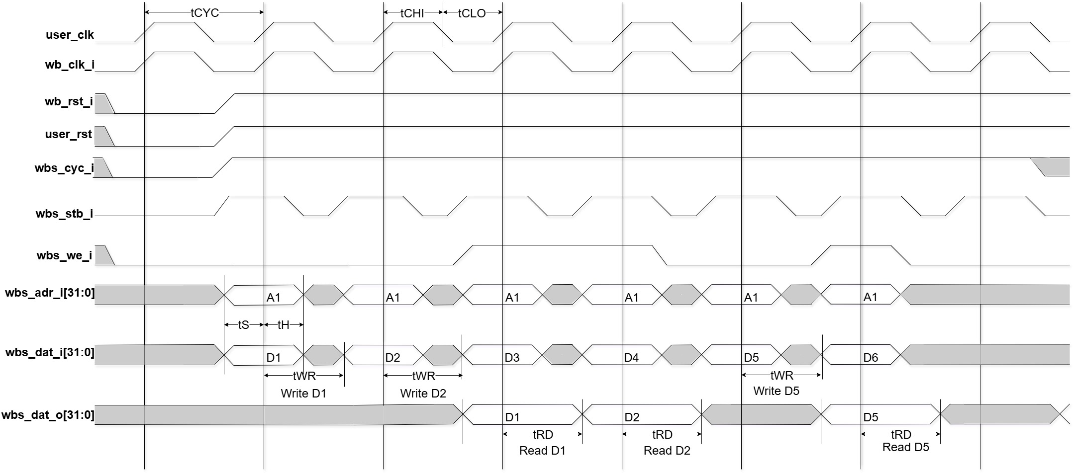
AC Specifications
Conditions
- Process Condition : Typical
- Junction Temperature : 25.000 deg C
- Operating Voltage : 1.800 V
- Operating Frequency : 1 MHz
Description
Symbol
Min Spec(ns)
Max Spec(ns)
Actual(ns)
Cycle Time
Tcyc
1000.000
Clock High Time
Tchi
500.000
Clock Low Time
Tclo
500.000
Clock to data-out (Read Cycle)
Trd
50.000
940.000
Rise: 520.000 Fall: 525.000
Clock to data-out (Write Cycle)
Twr
50.000
940.000
Rise: 510.000 Fall: 515.000
Setup time of addr/ctrl to clk
Tsad
500.000
Rise: 527.000 Fall: 617.000
Setup time of EN to clock
Tsen
800.000
850.000
Hold time of addr/ctrl from clk
Thad
300.000
Rise: 326.000 Fall: 325.000
Setup time of Data to clk
Tsdi
700.000
700.000
Hold time of data from clk
Thdi
1000.000
486.000
Setup time of BEN to clk
Tsben
700.000
821.000
Hold time of BEN from clk
Thben
1000.000
504.000
Test Mode Parameters
Description
Symbol
Min Spec(ns)
Max Spec(ns)
Actual(ns)
Clock to data-out (Test Mode)
Tcotm
50.000
900.000
Rise: 620.000
Fall: 635.000
Clock to ScanOutC (Test Mode)
Tcotm
50.000
900.000
Rise: 648.000
Fall: 645.000
Setup time of Add & Control to clk (Test Mode)
Tsctl_tm
800.000
Rise: 849.000
Fall: 878.000
Hold time of Add & Control from clk (Test Mode)
Thctl_tm
550.000
Rise: 574.000
Fall: 568.000
Setup time of TM, SM to clk
Tstm
650.000
650.000
Hold time of TM, SM from clk
Thtm
100.000
100.000
| Description | Symbol | Min Spec(ns) | Max Spec(ns) | Actual(ns) |
|---|---|---|---|---|
| Cycle Time | Tcyc | 1000.000 | ||
| Clock High Time | Tchi | 500.000 | ||
| Clock Low Time | Tclo | 500.000 | ||
| Clock to data-out (Read Cycle) | Trd | 50.000 | 940.000 | Rise: 520.000 Fall: 525.000 |
| Clock to data-out (Write Cycle) | Twr | 50.000 | 940.000 | Rise: 510.000 Fall: 515.000 |
| Setup time of addr/ctrl to clk | Tsad | 500.000 | Rise: 527.000 Fall: 617.000 | |
| Setup time of EN to clock | Tsen | 800.000 | 850.000 | |
| Hold time of addr/ctrl from clk | Thad | 300.000 | Rise: 326.000 Fall: 325.000 | |
| Setup time of Data to clk | Tsdi | 700.000 | 700.000 | |
| Hold time of data from clk | Thdi | 1000.000 | 486.000 | |
| Setup time of BEN to clk | Tsben | 700.000 | 821.000 | |
| Hold time of BEN from clk | Thben | 1000.000 | 504.000 |
| Description | Symbol | Min Spec(ns) | Max Spec(ns) | Actual(ns) |
|---|---|---|---|---|
| Clock to data-out (Test Mode) | Tcotm | 50.000 | 900.000 | Rise: 620.000 Fall: 635.000 |
| Clock to ScanOutC (Test Mode) | Tcotm | 50.000 | 900.000 | Rise: 648.000 Fall: 645.000 |
| Setup time of Add & Control to clk (Test Mode) | Tsctl_tm | 800.000 | Rise: 849.000 Fall: 878.000 |
|
| Hold time of Add & Control from clk (Test Mode) | Thctl_tm | 550.000 | Rise: 574.000 Fall: 568.000 |
|
| Setup time of TM, SM to clk | Tstm | 650.000 | 650.000 | |
| Hold time of TM, SM from clk | Thtm | 100.000 | 100.000 |
Timing Diagram